
Chinese Journal of Computational Physics ›› 2021, Vol. 38 ›› Issue (3): 361-370.DOI: 10.19596/j.cnki.1001-246x.8245
• Research Reports • Previous Articles Next Articles
Pengdi LI1,2( ), Jun LIU2,3, Qirong ZHENG2,3, Chuanguo ZHANG2,3, Yonggang LI2,3,*(), Yongsheng ZHANG2,3, Gaofeng ZHAO1,*(), Zhi ZENG2,3
Received:2020-06-22
Online:2021-05-25
Published:2021-09-30
Contact:
Yonggang LI, Gaofeng ZHAO
CLC Number:
Pengdi LI, Jun LIU, Qirong ZHENG, Chuanguo ZHANG, Yonggang LI, Yongsheng ZHANG, Gaofeng ZHAO, Zhi ZENG. Dynamics Modeling of Charged Defects in Si under B Ion Implantation[J]. Chinese Journal of Computational Physics, 2021, 38(3): 361-370.
Add to citation manager EndNote|Ris|BibTeX
URL: http://www.cjcp.org.cn/EN/10.19596/j.cnki.1001-246x.8245
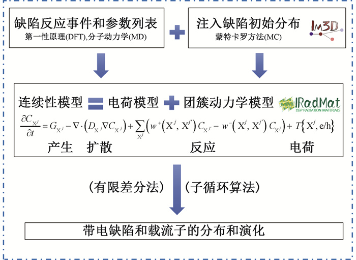
Fig.1 The framework of dynamic model of charged defects
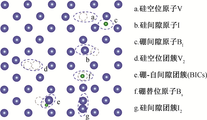
Fig.2 Schematic diagram of structure and location of defects in the continuum model
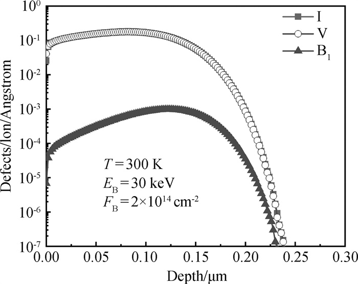
Fig.3 Depth distribution function of initial defects in Si under 30 keV B ion implantation simulated by IM3D
| 反应事件(不含团簇) | 反应事件(含团簇) |
| | |
| | |
| | |
| | |
| | |
| | |
| | |
| | |
| | |
| |
Table 1 Defect reaction events considered in the model
| 反应事件(不含团簇) | 反应事件(含团簇) |
| | |
| | |
| | |
| | |
| | |
| | |
| | |
| | |
| | |
| |
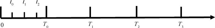
Fig.4 The distribution of time nodes in the sub-loop algorithmb
| 缺陷类型 | Ef/eV | D0/(cm2·s-1) | Em/eV | ΔEe/eV | ΔEh/eV | σe/cm2 | σh/cm2 | θ |
| I2- | 5.37 | 10-3 | 0.33 | 0.11 | 3×10-14 | |||
| I- | 4.61 | 10-3 | 0.54 | 0.26 | 1.01 | 3×10-16 | 3×10-14 | |
| I0 | 4.06 | 10-3 | 0.40 | 0.62 | 0.86 | 3×10-15 | 3×10-15 | |
| I+ | 3.73 | 10-3 | 0.37 | 0.47 | 0.50 | 3×10-14 | 3×10-16 | |
| I2+ | 3.68 | 10-3 | 1.10 | 0.65 | 3×10-14 | |||
| V2- | 4.33 | 1.5×10⁻² | 0.10 | 0.09 | 3×10-14 | |||
| V- | 3.87 | 1.3×10⁻³ | 0.19 | 0.40 | 1.03 | 3×10-16 | 3×10-14 | |
| V0 | 3.69 | 1.3×10⁻³ | 0.36 | 1.07 | 0.72 | 3×10-15 | 3×10-15 | |
| V+ | 4.07 | 9.6×10⁻³ | 0.44 | 0.99 | 0.05 | 3×10-14 | 3×10-16 | |
| V2+ | 4.55 | 9.6×10⁻³ | 0.71 | 0.13 | 3×10-14 | |||
| BS- | 0 | 1.075 | 3×10-14 | 1 | ||||
| BS0 | 0 | 0.045 | 1×10-20 | 4 | ||||
| BI- | 0.72 | 1.2×10⁻³ | 0.32 | 0.37 | 3×10-14 | |||
| BI0 | 0.63 | 1.2×10⁻³ | 0.40 | 0.13 | 0.75 | 3×10-15 | 3×10-15 | |
| BI+ | 1.13 | 1.2×10⁻³ | 0.95 | 0.99 | 3×10-14 | |||
| I2 | 6.52 | |||||||
| V2 | 5.57 | |||||||
| BI2 | 5.4 | |||||||
| B2 | 0.9 | |||||||
| BI2 | 2.2 | |||||||
| B2I2 | 4.4 |
Table 2 Physical parameters of defect and charge reactions in Si (Ef defect formation energy, D0 diffusion pre-exponential factor, Em migration energy, ΔEe/h activation energy for electron/hole emission, σe/h capture cross section, θ defect-state degeneracy.)
| 缺陷类型 | Ef/eV | D0/(cm2·s-1) | Em/eV | ΔEe/eV | ΔEh/eV | σe/cm2 | σh/cm2 | θ |
| I2- | 5.37 | 10-3 | 0.33 | 0.11 | 3×10-14 | |||
| I- | 4.61 | 10-3 | 0.54 | 0.26 | 1.01 | 3×10-16 | 3×10-14 | |
| I0 | 4.06 | 10-3 | 0.40 | 0.62 | 0.86 | 3×10-15 | 3×10-15 | |
| I+ | 3.73 | 10-3 | 0.37 | 0.47 | 0.50 | 3×10-14 | 3×10-16 | |
| I2+ | 3.68 | 10-3 | 1.10 | 0.65 | 3×10-14 | |||
| V2- | 4.33 | 1.5×10⁻² | 0.10 | 0.09 | 3×10-14 | |||
| V- | 3.87 | 1.3×10⁻³ | 0.19 | 0.40 | 1.03 | 3×10-16 | 3×10-14 | |
| V0 | 3.69 | 1.3×10⁻³ | 0.36 | 1.07 | 0.72 | 3×10-15 | 3×10-15 | |
| V+ | 4.07 | 9.6×10⁻³ | 0.44 | 0.99 | 0.05 | 3×10-14 | 3×10-16 | |
| V2+ | 4.55 | 9.6×10⁻³ | 0.71 | 0.13 | 3×10-14 | |||
| BS- | 0 | 1.075 | 3×10-14 | 1 | ||||
| BS0 | 0 | 0.045 | 1×10-20 | 4 | ||||
| BI- | 0.72 | 1.2×10⁻³ | 0.32 | 0.37 | 3×10-14 | |||
| BI0 | 0.63 | 1.2×10⁻³ | 0.40 | 0.13 | 0.75 | 3×10-15 | 3×10-15 | |
| BI+ | 1.13 | 1.2×10⁻³ | 0.95 | 0.99 | 3×10-14 | |||
| I2 | 6.52 | |||||||
| V2 | 5.57 | |||||||
| BI2 | 5.4 | |||||||
| B2 | 0.9 | |||||||
| BI2 | 2.2 | |||||||
| B2I2 | 4.4 |
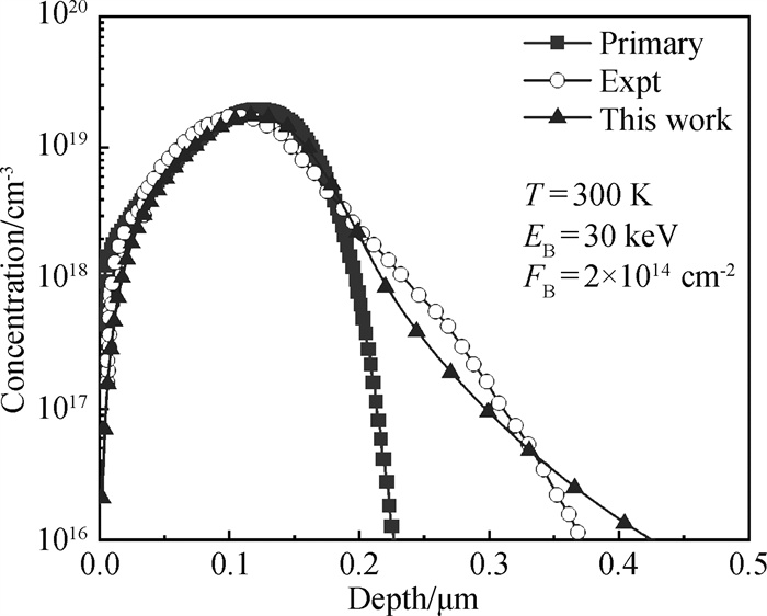
Fig.5 Depth distribution of B concentration in Si in simulation and experiment[4] under 30 keV B ion implantation with fluence of 2×1014 cm-2 at 300 K (Black line is the depth distribution of initial B concentration.)

Fig.6 Depth distributions of concentration of BI, BS and BICs after annealing to equilibrium at 300 K
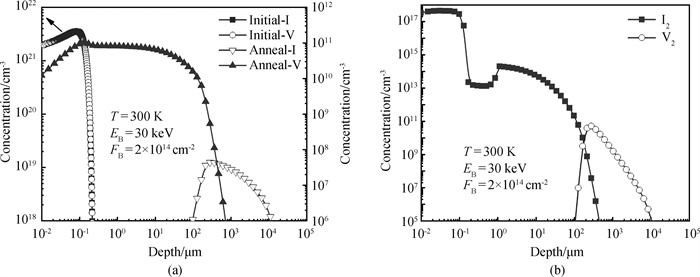
Fig.7 (a) Depth distributions of point defect concentration in Si before and after annealing to equilibrium; (b) Depth distributions of cluster concentration after annealing to equilibrium, under 30 keV B ion implantation with fluence of 2×1014 cm-2 at room temperature
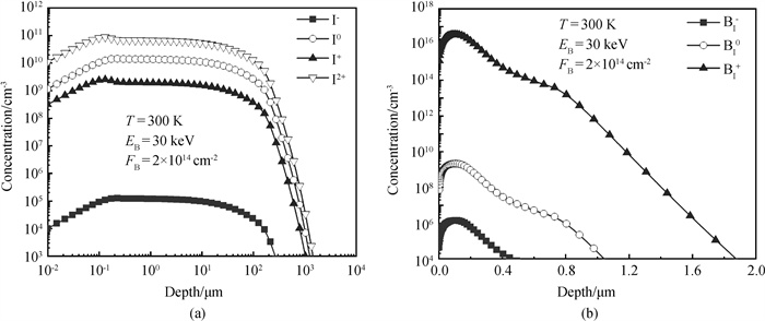
Fig.8 Depth distributions of the concentration of (a) I and (b) BI at different charge-state at 300 K
| 1 | PELAZ L, MARQUÉS L A, ABOY M, et al. Front-end process modeling in silicon[J]. Eur Phys J B, 2009, 72 (3): 323- 359. |
| 2 |
ZOGRAPHOS N, ZECHNERB C, IMARTIN-BRAGADOC G, et al. Multiscale modeling of doping processes in advanced semiconductor devices[J]. Mater Sci Semicond Process, 2017, 62, 49- 61.
DOI |
| 3 | YUAN G W, HANG X D, et al. Progress in numerical methods for radiation diffusion equations[J]. Chinese J Comput Phys, 2009, 26 (4): 475- 500. |
| 4 | ZHANG R, TANG Z P. Multiscale simulation of time and space in damage of a pre-tensioned aluminum plate under laser irradiation[J]. Chinese J Comput Phys, 2009, 26 (5): 743- 750. |
| 5 |
MATHIOT D, PFISTER J C. Dopant diffusion in silicon A consistent view involving nonequilibrium defects[J]. J Appl Phys, 1984, 55 (10): 3518.
DOI |
| 6 |
SOLMI S, BARUFFALDI F, CANTERI R. Diffusion of boron in silicon during post-implantation annealing[J]. J Appl Phys, 1991, 69 (4): 2135.
DOI |
| 7 |
COWERN N E, WALLE G F, ZALM P C, et al. Reactions of point defects and dopant atoms in silicon[J]. Phys Rev Lett, 1992, 69 (1): 116- 119.
DOI |
| 8 |
ZHU J, RUBIA T D D R, YANG L H Y. Ab initio pseudopotential calculations of B diffusion and pairing in Si[J]. Phys Rev B, 1996, 54 (7): 4741- 4747.
DOI |
| 9 |
SADIGH B, LENOSKY T J, THEISS S K, et al. Mechanism of boron diffusion in silicon: An ab initio and kinetic Monte Carlo study[J]. Phys Rev Lett, 1999, 83 (21): 4341- 4344.
DOI |
| 10 |
NAPOLITANI E, de SALVADOR D, STORTI R, et al. Room temperature migration of boron in crystalline silicon[J]. Phys Rev Lett, 2004, 93 (5): 055901.
DOI |
| 11 |
JÄGER H U. Point defect-based modeling of diffusion and electrical activation of ion implanted boron in crystalline silicon[J]. J Appl Phys, 1995, 78 (1): 176.
DOI |
| 12 |
FAHEY P M, GRIFFIN P B, PLUMMER J D. Point defects and dopant diffusion in silicon[J]. Rev Mod Phys, 1989, 61 (2): 289- 384.
DOI |
| 13 |
BACCUS B, WADA T, SHIGYO N. A study of nonequilibrium diffusion modeling-applications to rapid thermal annealing and advanced bipolar technologies[J]. IEEE Trans Electron Devices, 1992, 39 (3): 648.
DOI |
| 14 |
UEMATSU M. Simulation of boron, phosphorus, and arsenic diffusion in silicon based on an integrated diffusion model, and the anomalous phosphorus diffusion mechanism[J]. J Appl Phys, 1997, 82 (5): 2228.
DOI |
| 15 | PICHLER P. Intrinsic point defects, impurities, and their diffusion in silicon[M]. New York: Springer-Verlag Wien, 2004: 1- 554. |
| 16 |
ORTIZ C J, CRISTIANOB F, COLOMBEAU B. Modeling of extrinsic extended defect evolution in ion-implanted silicon upon thermal annealing[J]. Mater Sci Eng B, 2004, 114-115, 184- 192.
DOI |
| 17 |
MARTIN-BRAGADO I, CASTRILLO P, JARAIZ M, et al. Fermi-level effects in semiconductor processing: A modeling scheme for atomistic kinetic Monte Carlo simulators[J]. J Appl Phys, 2005, 98 (5): 053709.
DOI |
| 18 |
WINDL W, BUNEA M M, STUMPF R, et al. First principles study of boron diffusion in silicon[J]. Phys Rev Lett, 1999, 83 (21): 4345- 4348.
DOI |
| 19 |
CENTONI S A, SADIGH B, GILMER G H, et al. First principles calculation of intrinsic defect formation volumes in silicon[J]. Phys Rev B, 2005, 72 (19): 195206.
DOI |
| 20 | ZHANG J, ASHIZAWA Y, OKA H. Barrier to migration of the intrinsic defects in silicon in different charged system using First-principles calculations[J]. Mater Res Soc Symp Proc, 2005, 864, E9.17.1. |
| 21 |
WRIGHT A F. Density-functional-theory calculations for the silicon vacancy[J]. Phys Rev B, 2006, 74 (16): 165116.
DOI |
| 22 |
GANCHENKOVA M G, SUPRYADKINA I A, ABGARYAN K K, et al. Influence of the ab-initio calculation parameters on prediction of energy of point defects in silicon[J]. Modern Electronic Materials, 2015, 1, 103- 108.
DOI |
| 23 |
ABOY M, SANTOS I, PELAZ L, et al. Modeling of defects dopant diffusion and clustering in silicon[J]. J Comput Electron, 2014, 13 (1): 40- 58.
DOI |
| 24 | TANG P F, ZHENG Q R, LI Y G, et al. Cluster dynamics modeling with spatial correlations in cascades[J]. Chinese J Comput Phys, 2019, 36 (5): 586- 594. |
| 25 | LI Y G, ZHOU W H, NING R H, et al. A cluster dynamics model for accumulation of helium in tungsten under helium ions and neutron irradiation[J]. Prog Mater Sci, 2012, 11 (5): 1547- 1568. |
| 26 |
HU L, LI Y G, ZHANG C G, et al. Cluster dynamics simulation of deuterium retention behaviors in irradiated beryllium[J]. Rsc Advances, 2015, 5 (81): 65750- 65756.
DOI |
| 27 |
MARTIN-BRAGADO I, BORGES R, BALBUENA J P, et al. Kinetic Monte Carlo simulation for semiconductor processing: A review[J]. Prog Mater Sci, 2018, 92, 1- 32.
DOI |
| 28 |
SILLS R B AND CAI W. Efficient time integration in dislocation dynamics[J]. Modelling Simul Mater Sci Eng, 2014, 22 (2): 025003.
DOI |
| 29 |
LI Y G, YANG Y, SHORT M P, et al. IM3D: A parallel Monte Carlo code for efficient simulations of primary radiation displacements and damage in 3D geometry[J]. Sci Rep, 2015, 5, 18130.
DOI |
| 30 |
MYERS S M, COOPER P J, WAMPLER W R. Model of defect reactions and the influence of clustering in pulse-neutron-irradiated Si[J]. J Appl Phys, 2008, 104 (4): 044507.
DOI |
| 31 |
WAMPLER W R, MYERS S M. Model for transport and reaction of defects and carriers within displacement cascades in gallium arsenide[J]. J Appl Phys, 2015, 117 (4): 045707.
DOI |
| 32 | SEEBAUER E G, KRATZER M C. Charged point defects in semiconductors[J]. Mater Sci Eng R, 2006, 55, 51- 149. |
| 33 | JEONG J-W, OSHIYAMA A. Atomic and electronic structures of a boron impurity and its diffusion pathways in crystalline Si[J]. Phys Rev B, 2001, 64 (23): 235204. |
| 34 | SADIGH B, LENOSKY T J, THEISS S K. Mechanism of boron diffusion in silicon: An ab initio and kinetic Monte Carlo study[J]. Phys Rev Lett, 1999, 83 (21): 4341- 4344. |
| 35 | MIRABELLA S, DE SALVADOR D, NAPOLITANI E. Mechanisms of boron diffusion in silicon and germanium[J]. J Appl Phys, 2013, 113 (3): 031101. |
| [1] | YIN Haifeng, ZENG Chunhua, CHEN Wenjing. Plasmon Excitations in Two-dimensional Binary Silicon Carbide Nanostructures [J]. CHINESE JOURNAL OF COMPUTATIONAL PHYSICS, 2019, 36(5): 603-609. |
| [2] | MA Jianli, FU Zhifen, LI Yang, TANG Xudong, ZHANG Heming. Electron Mobility in Silicon Under Uniaxial[110] Stress [J]. CHINESE JOURNAL OF COMPUTATIONAL PHYSICS, 2017, 34(4): 483-488. |
| [3] | ZHOU Shuang, LIU Guili, JIANG Yan, SONG Yuanyuan. Adsorbing of Magnesium on Phosphorus-Doping Single-Walled Silicon Nanotubes: First-principles Study [J]. CHINESE JOURNAL OF COMPUTATIONAL PHYSICS, 2016, 33(5): 554-560. |
| [4] | LIU Futi, CHENG Yan, YANG Fubin, CHENG Xiaohong, CHEN Xlangrong. Electron Transport in Silicon Nanoscale Junctions [J]. CHINESE JOURNAL OF COMPUTATIONAL PHYSICS, 2013, 30(6): 943-948. |
| [5] | ZHANG Yan, DONG Gang, YANG Yintang, WANG Ning. Thermal Management of 3D Integrated Circuits Considering Horizontal Heat Transfer Effect [J]. CHINESE JOURNAL OF COMPUTATIONAL PHYSICS, 2013, 30(5): 753-758. |
| [6] | WANG Fengjuan, ZHU Zhangming, YANG Yintang, WANG Ning. A Thermal Model for Top Layer of Three-dimensional Integrated Circuits with Through Silicon Via [J]. CHINESE JOURNAL OF COMPUTATIONAL PHYSICS, 2012, 29(4): 580-584. |
| [7] | WANG Ping, YANG Yintang, LIU Zengji, SHANG Tao, Guo Lixin. Evaluation of DC I-V Characteristics and Small Signal Parameters of 4H-SiC Metal-Semiconductor Field Effect Transistors [J]. CHINESE JOURNAL OF COMPUTATIONAL PHYSICS, 2011, 28(1): 145-151. |
| [8] | SHENG Xiaowei, LUO Zhiyuan, CAI Qingdong. Numerical Study on Friction Between Solid Body and Granular Material [J]. CHINESE JOURNAL OF COMPUTATIONAL PHYSICS, 2009, 26(3): 403-408. |
| [9] | CHEN Wen-jian, XIE Jia-chun, XU Jun, HU Lin-hui, DONG Xiao-bo. The Coarse Dispersion of SiC/SiO2 Fractal Interface [J]. CHINESE JOURNAL OF COMPUTATIONAL PHYSICS, 2004, 21(4): 311-315. |
| [10] | YANG Lin-an, ZHANG Yi-men, YU Chun-li, YANG Yong-min, ZHANG Yu-ming. Surface-state Effects on Silicon Carbide Power MESFET's [J]. CHINESE JOURNAL OF COMPUTATIONAL PHYSICS, 2003, 20(5): 418-422. |
| [11] | MAN Zhen-yong, FENG Xi-qi. COMPUTER SIMULATIONS OF THE INTERACTIONS BETWEEN C20 AND A RECONSTRUCTED SILICON (100)-(2×1) SURFACE [J]. CHINESE JOURNAL OF COMPUTATIONAL PHYSICS, 2000, 17(S1): 65-70. |
| [12] | Min Xinmin, Deng Zhiping, Zhao Xiujian. STRUCTURES, PROPERTIES AND QUANTUM CHEMISTRY CALCULATING OF SILICON OXYNITRIDE AND OXIDE GLASSES [J]. CHINESE JOURNAL OF COMPUTATIONAL PHYSICS, 1997, 14(2): 242-246. |
| Viewed | ||||||
|
Full text |
|
|||||
|
Abstract |
|
|||||
Copyright © Chinese Journal of Computational Physics
E-mail: jswl@iapcm.ac.cn
Supported by Beijing Magtech Co., Ltd.