
计算物理 ›› 2021, Vol. 38 ›› Issue (3): 361-370.DOI: 10.19596/j.cnki.1001-246x.8245
李鹏迪1,2( ), 刘俊2,3, 郑淇蓉2,3, 张传国2,3, 李永钢2,3,*(), 张永胜2,3, 赵高峰1,*(), 曾雉2,3
收稿日期:2020-06-22
出版日期:2021-05-25
发布日期:2021-09-30
通讯作者:
李永钢,赵高峰
作者简介:李鹏迪(1995-), 女, 硕士研究生, 研究方向为半导体辐照的理论模拟, E-mail: pdli@theory.issp.ac.cn
基金资助:
Pengdi LI1,2(), Jun LIU2,3, Qirong ZHENG2,3, Chuanguo ZHANG2,3, Yonggang LI2,3,*(), Yongsheng ZHANG2,3, Gaofeng ZHAO1,*(), Zhi ZENG2,3
Received:2020-06-22
Online:2021-05-25
Published:2021-09-30
Contact:
Yonggang LI, Gaofeng ZHAO
摘要:
为准确描述硼离子注入硅后缺陷/杂质的动力学物理过程,获得硼浓度空间分布及其演化行为,构建一个跨尺度带电缺陷动力学模型,考虑离子注入缺陷的产生及其演化的多种微观过程,包括缺陷电荷态和带电缺陷间的反应、硼-自间隙团簇(BICs)演化以及缺陷与载流子相互作用等物理过程。模拟得到与实验一致的硼浓度深度分布。结果表明:BICs对硼浓度的深度分布起主要作用,而间隙硼(BI)导致硼浓度分布向深处扩展;计及缺陷的不同电荷态修正自间隙(I)和硼间隙(BI)的扩散系数,从而更准确地描述硼浓度分布。模型揭示了硼离子注入硅发生的物理过程和微观机理,证明BICs和缺陷真实的电荷态是描述硼浓度分布的重要因素,为半导体器件制造与研发提供理论指导。
中图分类号:
李鹏迪, 刘俊, 郑淇蓉, 张传国, 李永钢, 张永胜, 赵高峰, 曾雉. 硅中硼离子注入的带电缺陷动力学模拟[J]. 计算物理, 2021, 38(3): 361-370.
Pengdi LI, Jun LIU, Qirong ZHENG, Chuanguo ZHANG, Yonggang LI, Yongsheng ZHANG, Gaofeng ZHAO, Zhi ZENG. Dynamics Modeling of Charged Defects in Si under B Ion Implantation[J]. Chinese Journal of Computational Physics, 2021, 38(3): 361-370.
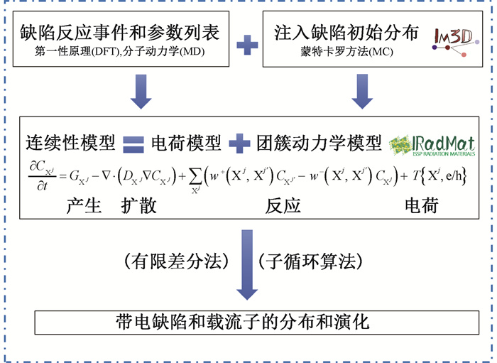
图1 带电缺陷动力学模型框架
Fig.1 The framework of dynamic model of charged defects
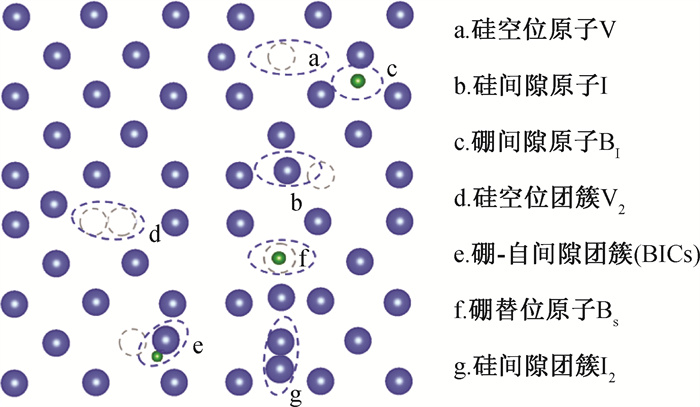
图2 连续性模型中缺陷的结构和位置示意图
Fig.2 Schematic diagram of structure and location of defects in the continuum model
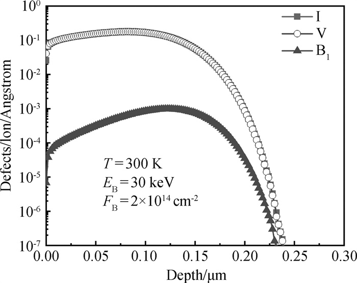
图3 IM3D模拟的30 keV硼离子注入硅的初始缺陷深度分布函数
Fig.3 Depth distribution function of initial defects in Si under 30 keV B ion implantation simulated by IM3D
| 反应事件(不含团簇) | 反应事件(含团簇) |
| | |
| | |
| | |
| | |
| | |
| | |
| | |
| | |
| | |
| |
表1 模型中考虑的缺陷反应事件
Table 1 Defect reaction events considered in the model
| 反应事件(不含团簇) | 反应事件(含团簇) |
| | |
| | |
| | |
| | |
| | |
| | |
| | |
| | |
| | |
| |
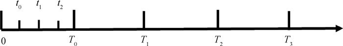
图4 子循环算法的时间节点分布
Fig.4 The distribution of time nodes in the sub-loop algorithmb
| 缺陷类型 | Ef/eV | D0/(cm2·s-1) | Em/eV | ΔEe/eV | ΔEh/eV | σe/cm2 | σh/cm2 | θ |
| I2- | 5.37 | 10-3 | 0.33 | 0.11 | 3×10-14 | |||
| I- | 4.61 | 10-3 | 0.54 | 0.26 | 1.01 | 3×10-16 | 3×10-14 | |
| I0 | 4.06 | 10-3 | 0.40 | 0.62 | 0.86 | 3×10-15 | 3×10-15 | |
| I+ | 3.73 | 10-3 | 0.37 | 0.47 | 0.50 | 3×10-14 | 3×10-16 | |
| I2+ | 3.68 | 10-3 | 1.10 | 0.65 | 3×10-14 | |||
| V2- | 4.33 | 1.5×10⁻² | 0.10 | 0.09 | 3×10-14 | |||
| V- | 3.87 | 1.3×10⁻³ | 0.19 | 0.40 | 1.03 | 3×10-16 | 3×10-14 | |
| V0 | 3.69 | 1.3×10⁻³ | 0.36 | 1.07 | 0.72 | 3×10-15 | 3×10-15 | |
| V+ | 4.07 | 9.6×10⁻³ | 0.44 | 0.99 | 0.05 | 3×10-14 | 3×10-16 | |
| V2+ | 4.55 | 9.6×10⁻³ | 0.71 | 0.13 | 3×10-14 | |||
| BS- | 0 | 1.075 | 3×10-14 | 1 | ||||
| BS0 | 0 | 0.045 | 1×10-20 | 4 | ||||
| BI- | 0.72 | 1.2×10⁻³ | 0.32 | 0.37 | 3×10-14 | |||
| BI0 | 0.63 | 1.2×10⁻³ | 0.40 | 0.13 | 0.75 | 3×10-15 | 3×10-15 | |
| BI+ | 1.13 | 1.2×10⁻³ | 0.95 | 0.99 | 3×10-14 | |||
| I2 | 6.52 | |||||||
| V2 | 5.57 | |||||||
| BI2 | 5.4 | |||||||
| B2 | 0.9 | |||||||
| BI2 | 2.2 | |||||||
| B2I2 | 4.4 |
表2 缺陷和电荷反应物理参数(Ef为缺陷形成能,D0为扩散前置因子,Em为扩散迁移能,ΔEe/h为发射电子/空穴所需激活能,σe/h为缺陷捕获电子/空穴截面,θ为电荷态简并度。)
Table 2 Physical parameters of defect and charge reactions in Si (Ef defect formation energy, D0 diffusion pre-exponential factor, Em migration energy, ΔEe/h activation energy for electron/hole emission, σe/h capture cross section, θ defect-state degeneracy.)
| 缺陷类型 | Ef/eV | D0/(cm2·s-1) | Em/eV | ΔEe/eV | ΔEh/eV | σe/cm2 | σh/cm2 | θ |
| I2- | 5.37 | 10-3 | 0.33 | 0.11 | 3×10-14 | |||
| I- | 4.61 | 10-3 | 0.54 | 0.26 | 1.01 | 3×10-16 | 3×10-14 | |
| I0 | 4.06 | 10-3 | 0.40 | 0.62 | 0.86 | 3×10-15 | 3×10-15 | |
| I+ | 3.73 | 10-3 | 0.37 | 0.47 | 0.50 | 3×10-14 | 3×10-16 | |
| I2+ | 3.68 | 10-3 | 1.10 | 0.65 | 3×10-14 | |||
| V2- | 4.33 | 1.5×10⁻² | 0.10 | 0.09 | 3×10-14 | |||
| V- | 3.87 | 1.3×10⁻³ | 0.19 | 0.40 | 1.03 | 3×10-16 | 3×10-14 | |
| V0 | 3.69 | 1.3×10⁻³ | 0.36 | 1.07 | 0.72 | 3×10-15 | 3×10-15 | |
| V+ | 4.07 | 9.6×10⁻³ | 0.44 | 0.99 | 0.05 | 3×10-14 | 3×10-16 | |
| V2+ | 4.55 | 9.6×10⁻³ | 0.71 | 0.13 | 3×10-14 | |||
| BS- | 0 | 1.075 | 3×10-14 | 1 | ||||
| BS0 | 0 | 0.045 | 1×10-20 | 4 | ||||
| BI- | 0.72 | 1.2×10⁻³ | 0.32 | 0.37 | 3×10-14 | |||
| BI0 | 0.63 | 1.2×10⁻³ | 0.40 | 0.13 | 0.75 | 3×10-15 | 3×10-15 | |
| BI+ | 1.13 | 1.2×10⁻³ | 0.95 | 0.99 | 3×10-14 | |||
| I2 | 6.52 | |||||||
| V2 | 5.57 | |||||||
| BI2 | 5.4 | |||||||
| B2 | 0.9 | |||||||
| BI2 | 2.2 | |||||||
| B2I2 | 4.4 |
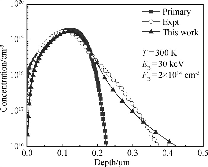
图5 300 K下,注入量为2×1014 cm-2的30 keV硼离子注入硅后硼浓度深度分布的模拟与实验结果[4]
Fig.5 Depth distribution of B concentration in Si in simulation and experiment[4] under 30 keV B ion implantation with fluence of 2×1014 cm-2 at 300 K (Black line is the depth distribution of initial B concentration.)

图6 300 K下退火至平衡时BI、BS以及BICs的深度分布
Fig.6 Depth distributions of concentration of BI, BS and BICs after annealing to equilibrium at 300 K
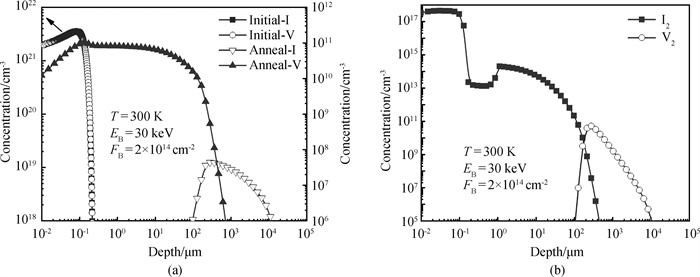
图7 (a) 30 keV,2×1014 cm-2硼离子注入硅, 初始时刻和常温退火后点缺陷深度分布;(b) 常温退火后点缺陷团簇的浓度分布
Fig.7 (a) Depth distributions of point defect concentration in Si before and after annealing to equilibrium; (b) Depth distributions of cluster concentration after annealing to equilibrium, under 30 keV B ion implantation with fluence of 2×1014 cm-2 at room temperature
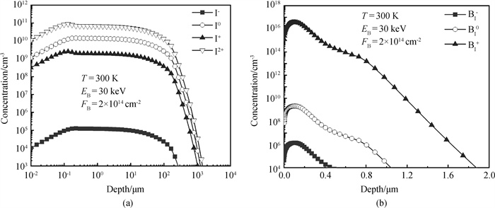
图8 300 K下退火后不同电荷态(a) I和(b) BI浓度的深度分布
Fig.8 Depth distributions of the concentration of (a) I and (b) BI at different charge-state at 300 K
| 1 | PELAZ L, MARQUÉS L A, ABOY M, et al. Front-end process modeling in silicon[J]. Eur Phys J B, 2009, 72 (3): 323- 359. |
| 2 |
ZOGRAPHOS N, ZECHNERB C, IMARTIN-BRAGADOC G, et al. Multiscale modeling of doping processes in advanced semiconductor devices[J]. Mater Sci Semicond Process, 2017, 62, 49- 61.
DOI |
| 3 | YUAN G W, HANG X D, et al. Progress in numerical methods for radiation diffusion equations[J]. Chinese J Comput Phys, 2009, 26 (4): 475- 500. |
| 4 | ZHANG R, TANG Z P. Multiscale simulation of time and space in damage of a pre-tensioned aluminum plate under laser irradiation[J]. Chinese J Comput Phys, 2009, 26 (5): 743- 750. |
| 5 |
MATHIOT D, PFISTER J C. Dopant diffusion in silicon A consistent view involving nonequilibrium defects[J]. J Appl Phys, 1984, 55 (10): 3518.
DOI |
| 6 |
SOLMI S, BARUFFALDI F, CANTERI R. Diffusion of boron in silicon during post-implantation annealing[J]. J Appl Phys, 1991, 69 (4): 2135.
DOI |
| 7 |
COWERN N E, WALLE G F, ZALM P C, et al. Reactions of point defects and dopant atoms in silicon[J]. Phys Rev Lett, 1992, 69 (1): 116- 119.
DOI |
| 8 |
ZHU J, RUBIA T D D R, YANG L H Y. Ab initio pseudopotential calculations of B diffusion and pairing in Si[J]. Phys Rev B, 1996, 54 (7): 4741- 4747.
DOI |
| 9 |
SADIGH B, LENOSKY T J, THEISS S K, et al. Mechanism of boron diffusion in silicon: An ab initio and kinetic Monte Carlo study[J]. Phys Rev Lett, 1999, 83 (21): 4341- 4344.
DOI |
| 10 |
NAPOLITANI E, de SALVADOR D, STORTI R, et al. Room temperature migration of boron in crystalline silicon[J]. Phys Rev Lett, 2004, 93 (5): 055901.
DOI |
| 11 |
JÄGER H U. Point defect-based modeling of diffusion and electrical activation of ion implanted boron in crystalline silicon[J]. J Appl Phys, 1995, 78 (1): 176.
DOI |
| 12 |
FAHEY P M, GRIFFIN P B, PLUMMER J D. Point defects and dopant diffusion in silicon[J]. Rev Mod Phys, 1989, 61 (2): 289- 384.
DOI |
| 13 |
BACCUS B, WADA T, SHIGYO N. A study of nonequilibrium diffusion modeling-applications to rapid thermal annealing and advanced bipolar technologies[J]. IEEE Trans Electron Devices, 1992, 39 (3): 648.
DOI |
| 14 |
UEMATSU M. Simulation of boron, phosphorus, and arsenic diffusion in silicon based on an integrated diffusion model, and the anomalous phosphorus diffusion mechanism[J]. J Appl Phys, 1997, 82 (5): 2228.
DOI |
| 15 | PICHLER P. Intrinsic point defects, impurities, and their diffusion in silicon[M]. New York: Springer-Verlag Wien, 2004: 1- 554. |
| 16 |
ORTIZ C J, CRISTIANOB F, COLOMBEAU B. Modeling of extrinsic extended defect evolution in ion-implanted silicon upon thermal annealing[J]. Mater Sci Eng B, 2004, 114-115, 184- 192.
DOI |
| 17 |
MARTIN-BRAGADO I, CASTRILLO P, JARAIZ M, et al. Fermi-level effects in semiconductor processing: A modeling scheme for atomistic kinetic Monte Carlo simulators[J]. J Appl Phys, 2005, 98 (5): 053709.
DOI |
| 18 |
WINDL W, BUNEA M M, STUMPF R, et al. First principles study of boron diffusion in silicon[J]. Phys Rev Lett, 1999, 83 (21): 4345- 4348.
DOI |
| 19 |
CENTONI S A, SADIGH B, GILMER G H, et al. First principles calculation of intrinsic defect formation volumes in silicon[J]. Phys Rev B, 2005, 72 (19): 195206.
DOI |
| 20 | ZHANG J, ASHIZAWA Y, OKA H. Barrier to migration of the intrinsic defects in silicon in different charged system using First-principles calculations[J]. Mater Res Soc Symp Proc, 2005, 864, E9.17.1. |
| 21 |
WRIGHT A F. Density-functional-theory calculations for the silicon vacancy[J]. Phys Rev B, 2006, 74 (16): 165116.
DOI |
| 22 |
GANCHENKOVA M G, SUPRYADKINA I A, ABGARYAN K K, et al. Influence of the ab-initio calculation parameters on prediction of energy of point defects in silicon[J]. Modern Electronic Materials, 2015, 1, 103- 108.
DOI |
| 23 |
ABOY M, SANTOS I, PELAZ L, et al. Modeling of defects dopant diffusion and clustering in silicon[J]. J Comput Electron, 2014, 13 (1): 40- 58.
DOI |
| 24 | TANG P F, ZHENG Q R, LI Y G, et al. Cluster dynamics modeling with spatial correlations in cascades[J]. Chinese J Comput Phys, 2019, 36 (5): 586- 594. |
| 25 | LI Y G, ZHOU W H, NING R H, et al. A cluster dynamics model for accumulation of helium in tungsten under helium ions and neutron irradiation[J]. Prog Mater Sci, 2012, 11 (5): 1547- 1568. |
| 26 |
HU L, LI Y G, ZHANG C G, et al. Cluster dynamics simulation of deuterium retention behaviors in irradiated beryllium[J]. Rsc Advances, 2015, 5 (81): 65750- 65756.
DOI |
| 27 |
MARTIN-BRAGADO I, BORGES R, BALBUENA J P, et al. Kinetic Monte Carlo simulation for semiconductor processing: A review[J]. Prog Mater Sci, 2018, 92, 1- 32.
DOI |
| 28 |
SILLS R B AND CAI W. Efficient time integration in dislocation dynamics[J]. Modelling Simul Mater Sci Eng, 2014, 22 (2): 025003.
DOI |
| 29 |
LI Y G, YANG Y, SHORT M P, et al. IM3D: A parallel Monte Carlo code for efficient simulations of primary radiation displacements and damage in 3D geometry[J]. Sci Rep, 2015, 5, 18130.
DOI |
| 30 |
MYERS S M, COOPER P J, WAMPLER W R. Model of defect reactions and the influence of clustering in pulse-neutron-irradiated Si[J]. J Appl Phys, 2008, 104 (4): 044507.
DOI |
| 31 |
WAMPLER W R, MYERS S M. Model for transport and reaction of defects and carriers within displacement cascades in gallium arsenide[J]. J Appl Phys, 2015, 117 (4): 045707.
DOI |
| 32 | SEEBAUER E G, KRATZER M C. Charged point defects in semiconductors[J]. Mater Sci Eng R, 2006, 55, 51- 149. |
| 33 | JEONG J-W, OSHIYAMA A. Atomic and electronic structures of a boron impurity and its diffusion pathways in crystalline Si[J]. Phys Rev B, 2001, 64 (23): 235204. |
| 34 | SADIGH B, LENOSKY T J, THEISS S K. Mechanism of boron diffusion in silicon: An ab initio and kinetic Monte Carlo study[J]. Phys Rev Lett, 1999, 83 (21): 4341- 4344. |
| 35 | MIRABELLA S, DE SALVADOR D, NAPOLITANI E. Mechanisms of boron diffusion in silicon and germanium[J]. J Appl Phys, 2013, 113 (3): 031101. |
| [1] | 尹海峰, 曾春花, 陈文经. 二维二元碳化硅纳米结构的等离激元激发[J]. 计算物理, 2019, 36(5): 603-609. |
| [2] | 王凤娟, 王刚, 余宁梅. 同轴-环形TSV电学性能[J]. 计算物理, 2018, 35(2): 242-252. |
| [3] | 马建立, 付志粉, 李洋, 唐旭东, 张鹤鸣. 单轴[110]应力硅电子迁移率[J]. 计算物理, 2017, 34(4): 483-488. |
| [4] | 周爽, 刘贵立, 姜艳, 宋媛媛. P掺杂单壁硅纳米管Mg原子吸附性能的第一性原理研究[J]. 计算物理, 2016, 33(5): 554-560. |
| [5] | 柳福提, 程艳, 羊富彬, 程晓洪, 陈向荣. 硅纳米结点电子输运性质的计算[J]. 计算物理, 2013, 30(6): 943-948. |
| [6] | 张岩, 董刚, 杨银堂, 王宁. 考虑通孔横向热传输效应的三维集成电路热分析[J]. 计算物理, 2013, 30(5): 753-758. |
| [7] | 马海珠, 林敏, 陈禹宏, 刘倩, 江谦. 聚有机硅结构和规整性对链柔性和极性的影响[J]. 计算物理, 2013, 30(3): 447-453. |
| [8] | 王凤娟, 朱樟明, 杨银堂, 王宁. 考虑硅通孔的三维集成电路最高层温度模型[J]. 计算物理, 2012, 29(4): 580-584. |
| [9] | 吕少波, 蔺增, 巴德纯, 王庆. 射频辉光放电CH4等离子体一维流体动力学模拟[J]. 计算物理, 2011, 28(3): 329-340. |
| [10] | 王平, 杨银堂, 刘增基, 尚韬, 郭立新. 4H-SiC金属-半导体场效应晶体管大信号I-V特性和小信号参数的计算[J]. 计算物理, 2011, 28(1): 145-151. |
| [11] | 丁瑞雪, 杨银堂, 刘帘曦. 新型NO2化学传感器:碳化硅纳米管[J]. 计算物理, 2010, 27(5): 779-784. |
| [12] | 沈海军, 史友进. 加氢单壁硅纳米管的热稳定性与拉伸力学特性[J]. 计算物理, 2008, 25(1): 92-96. |
| [13] | 王平, 杨银堂, 杨燕. SiC电子霍耳迁移率的计算[J]. 计算物理, 2006, 23(1): 80-86. |
| [14] | 王平, 杨银堂, 屈汉章, 杨燕, 李跃进, 贾护军. SiC电子输运特性的Monte Carlo数值模拟[J]. 计算物理, 2005, 22(3): 245-250. |
| [15] | 杨林安, 张义门, 于春利, 杨永民, 张玉明. 表面态对碳化硅功率金-半场效应管特性的影响[J]. 计算物理, 2003, 20(5): 418-422. |
| 阅读次数 | ||||||
|
全文 |
|
|||||
|
摘要 |
|
|||||
版权所有 © 《计算物理》编辑部
地址:北京市海淀区丰豪东路2号 邮编:100094 E-mail:jswl@iapcm.ac.cn
本系统由北京玛格泰克科技发展有限公司设计开发